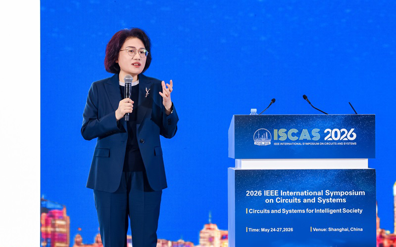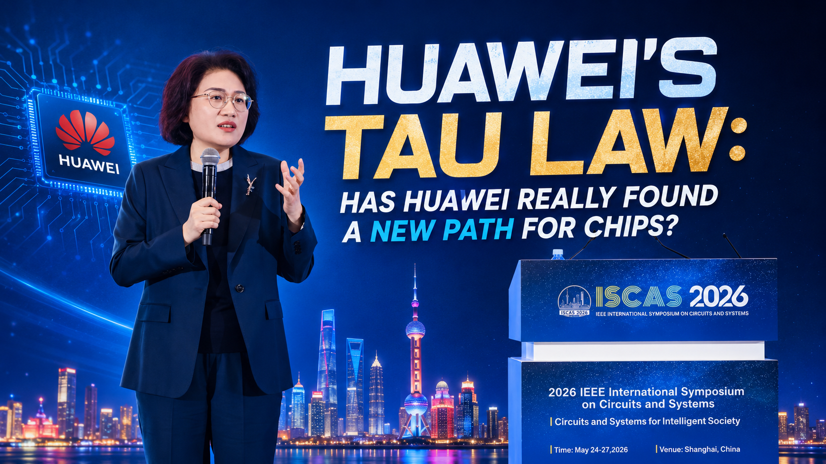
Recently, a new term has been spreading across Chinese tech circles: τ Law, also called Tau Law. It became a hot topic after Huawei presented it as a possible new direction for semiconductor development.
For many years, the chip industry has followed one main rule: make transistors smaller. This is the logic behind Moore’s Law. A smaller process node, such as 7nm, 5nm, or 3nm, usually means better performance, lower power consumption, and more transistors packed into the same chip area. Companies like TSMC, Samsung, Intel, Apple, and Nvidia have all benefited from this race.
But Huawei’s situation is different.
Because of technology restrictions, Huawei cannot easily access the most advanced chipmaking equipment, especially EUV lithography machines. This makes it difficult for Huawei to compete directly in the traditional “smaller nanometer” race.
So Huawei is trying to tell a different story: maybe the future of chips is not only about making transistors smaller. Maybe it is also about making the whole chip system more efficient.
That is where Tau Law comes in.
In electronics, τ, or tau, is related to the delay of electrical signals. A simple way to understand it is:
τ = R × C
Here, R means resistance, and C means capacitance. The larger the tau value, the slower signals may travel inside the chip. The smaller the tau value, the faster the circuit can respond.
Huawei’s idea is that chip performance can be improved by reducing this signal delay. Instead of only focusing on transistor size, engineers can improve chip speed by redesigning the architecture, shortening signal paths, improving interconnects, and optimizing the relationship between software, hardware, and system design.
In simple words:
Traditional chip development says:
“Make the transistors smaller.”
Huawei’s Tau Law says:
“Make the whole chip communicate faster and work more efficiently.”
This is why some people see Huawei’s idea as a possible new route. It does not completely replace advanced manufacturing, but it may help Huawei reduce the gap when it cannot use the most advanced production technology.
Huawei has also mentioned related ideas such as LogicFolding, system-level chip design, and full-stack optimization. These sound technical, but the main point is simple: Huawei wants to improve performance by changing how the chip is designed and how different parts of the system work together.
This is important because modern chips are no longer limited only by transistor size. As chips become more complex, internal communication becomes a major challenge. A chip may have billions of transistors, but if data moves slowly between different parts, overall performance is still limited.
So, from a technical point of view, Huawei’s direction makes sense. Signal delay, power consumption, and system architecture are real problems in the semiconductor industry.
However, we should also be careful.
Tau Law is not magic. It does not mean Huawei can suddenly defeat TSMC, Nvidia, or Apple overnight. Advanced manufacturing is still extremely important. Smaller process nodes still bring real advantages in density, power efficiency, and performance.
The key question is not whether Huawei’s idea sounds interesting. The real question is whether Huawei can prove it with real products.
This is where the next Huawei flagship becomes important.
Huawei has reportedly said that this new approach could be implemented before the end of this year. Many people believe the first major showcase could be the next flagship Huawei Mate 90 series, possibly powered by a new Kirin chipset designed around this Tau Law or LogicFolding approach.
If that happens, the Mate 90 will not just be another smartphone launch. It could become a real-world test of Huawei’s new chip strategy.
Instead of only talking about theory, Huawei would finally have to prove whether this architecture can bring meaningful improvements in performance, power efficiency, heat control, AI capability, and daily user experience.
This is why the next Kirin chip matters so much.
If it performs well, Huawei can show that it has found a practical way to improve chips even without relying fully on the most advanced manufacturing process. It would prove that better architecture, better system design, and smarter optimization can still create real progress.
But if the improvement is small, then Tau Law may be seen more as a clever technical narrative than a true breakthrough.
In my opinion, Huawei’s Tau Law is best understood as a strategic response to a difficult situation. Since Huawei cannot easily follow the same path as global chip giants, it is trying to create another path: one based on architecture, system design, and efficiency.
This does not mean the old chip race is over. But it does show that the semiconductor industry may be entering a more complex era. Future progress may not come only from smaller nanometers. It may also come from smarter design.
So, has Huawei found a new path?
For my opinion is YES! But the real answer will come when the new Kirin chip reaches consumers. If the Mate 90 launches with this technology before the end of the year, it may become one of the most important Huawei products in recent years — not just because of the phone itself, but because it will show whether Huawei’s alternative semiconductor path can actually work in the real world.
For now, Tau Law is not a final victory. It is Huawei’s attempt to turn limitation into innovation.
Whether it becomes a real breakthrough will depend on what Huawei delivers next.